
Power semiconductor device
Power semiconductor devices are semiconductor devices used as switches or rectifiers in power electronic circuits (switch mode power supplies for example). They are also called power devices or when used in integrated circuits, called power ICs.
Most power semiconductor devices are only used in commutation mode (i.e they are either on or off), and are therefore optimized for this. Most of them should not be used in linear operation.
Most power semiconductor devices are only used in commutation mode (i.e they are either on or off), and are therefore optimized for this. Most of them should not be used in linear operation.
History
Power semiconductor devices first appeared in 1952 with the introduction of the power diode by R.N. Hall. It was made of Germanium and had a voltage capability of 200 volts and a current rating of 35 amperes.
The thyristor appeared in 1957. Thyristors are able to withstand very high reverse breakdown voltage and are also capable of carrying high current. One disadvantage of the thyristor for switching circuits is that once it is 'latched-on' in the conducting state it cannot be turned off by external control. The thyristor turn-off is passive, i.e., the power must be disconnected from the device.
The first bipolar transistors devices with substantial power handling capabilities were introduced in the 1960s. These components overcame some limitations of the thyristors because they can be turned on or off with an applied signal.
With the improvements of the Metal Oxide Semiconductor technology (initially developed to produce integrated circuits), power MOSFETs became available in the late 1970s. International Rectifier introduced a 25 A, 400 V power MOSFET in 1978. These devices allow operation at higher frequency than bipolar transistors, but are limited to the low voltage applications.
The Insulated Gate Bipolar Transistor (IGBT) developed in the 1980s became widely available in the 1990s. This component has the power handling capability of the bipolar transistor, with the advantages of the isolated gate drive of the power MOSFET.
Common power devices
Some common power devices are the power diode, thyristor, power MOSFET and IGBT. A power diode or MOSFET operates on similar principles to its low-power counterpart, but is able to carry a larger amount of current and typically is able to support a larger reverse-bias voltage in the off-state.
Structural changes are often made in power devices to accommodate the higher current density, higher power dissipation and/or higher reverse breakdown voltage. The vast majority of the discrete (i.e non integrated) power devices are built using a vertical structure, whereas small-signal devices employ a lateral structure. With the vertical structure, the current rating of the device is proportional to its area, and the voltage blocking capability is achieved in the height of the die. With this structure, one of the connections of the device is located on the bottom of the semiconductor die.
Structural changes are often made in power devices to accommodate the higher current density, higher power dissipation and/or higher reverse breakdown voltage. The vast majority of the discrete (i.e non integrated) power devices are built using a vertical structure, whereas small-signal devices employ a lateral structure. With the vertical structure, the current rating of the device is proportional to its area, and the voltage blocking capability is achieved in the height of the die. With this structure, one of the connections of the device is located on the bottom of the semiconductor die.
Common power semiconductor devices
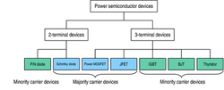
The realm of power devices is divided into two main categories (see figure 1):
- The two-terminal devices (diodes), whose state is completely dependent on the external power circuit they are connected to;
- The three-terminal devices, whose state is not only dependent on their external power circuit, but also on the signal on their driving terminal (gate or base). Transistors and thyristors belong to that category.
Diodes
An ideal diode should have the following characteristics:
This trade-off between on-state/off-state and switching speed is the same for all power devices. A Schottky diode has excellent switching speed and on-state performance, but a high level of leakage current in off-state. On the other hand, PIN diodes are commercially available in different commutation speeds (so-called "fast" and "ultrafast" rectifiers), but any increase in speed is paid for by a lower performance in the on-state.
- When forward-biased, the voltage across the end terminals of the diode should be zero, whatever the current that flows through it (on-state);
- When reverse-biased, the leakage current should be zero, whatever the voltage (off-state).
- The transition between on and off states should be instantaneous.
This trade-off between on-state/off-state and switching speed is the same for all power devices. A Schottky diode has excellent switching speed and on-state performance, but a high level of leakage current in off-state. On the other hand, PIN diodes are commercially available in different commutation speeds (so-called "fast" and "ultrafast" rectifiers), but any increase in speed is paid for by a lower performance in the on-state.
Switches
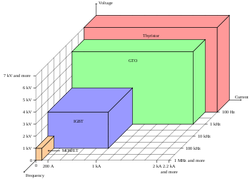
The trade-off between voltage, current and frequency ratings also exists for the switches. Actually, all power semiconductors rely on a PIN diode structure to sustain voltage. This can be seen in figure 2. The power MOSFET has the advantages of the majority carrier devices, so it can achieve very high operating frequency, but can't be used with high voltages. As it is a physical limit, no improvement is expected from siliconMOSFETs concerning their maximum voltage ratings. However, its excellent performance in low voltage make it the device of choice (actually the only choice) for applications below 200 V. By paralleling several devices, it is possible to increase the current rating of a switch. The MOSFET is particularly suited to this configuration because its positive thermal coefficient of resistance tends to balance current between individual devices.
The IGBT is a recent component, so its performance improves regularly as technology evolves. It has already completely replaced the bipolar transistor in power applications, and the availability of power modules (in which several IGBT dice are connected in parallel) makes it attractive for power levels up to several megawatts, pushing further the limit where thyristors and GTOs become the only option. Basically, an IGBT is a bipolar transistor driven by a power MOSFET: it has the advantages of being a minority carrier device (good performance in on-state, even for high voltage devices), with the high input impedance of a MOSFET (it can be driven on or off with a very low amount of power). Its major limitation for low voltage applications is the high voltage drop it exhibits in on-state (2 to 4 V). Compared to the MOSFET, the operating frequency of the IGBT is relatively low (few devices are rated over 50 kHz), mainly because of a so-called 'current-tail' problem during turn-off. This problem is caused by the slow decay of the conduction current during turn-off resulting from slow recombination of large number of carriers, which flood the thick 'drift' region of the IGBT during conduction. The net result is that the turn-off switching loss of an IGBT is considerably higher than its turn-on loss. Generally, in datasheets, turn-off energy is mentioned as a measured parameter and one has to multiply that number with the switching frequency of the intended application to estimate the turn-off loss.
At very high power levels, thyristor-based devices (SCRs, GTOs, MCTs) are still the only choice. Though driving a thyristor is somewhat complicated, as this device can only be turned on. It turns off by itself as soon as no more current flows through it. This requires a circuit with the means to divert current, or specific applications where current is known to drop to zero regularly (i.e. Alternating Current). MCTs and GTOs have been developed to overcome this limitation; these components are widely used in power distribution applications.
Parameters of power semiconductor devices
- Breakdown voltage: Often there is a trade-off between breakdown voltage rating and on-resistance, because increasing the breakdown voltage by incorporating a thicker and lower doped drift region leads to higher on-resistance.
- On-resistance: Higher current rating lowers the on-resistance due to greater numbers of parallel cells. This increases overall capacitance and slows down the speed.
- Rise and fall times for switching between on and off states.
- Safe-operating area (from thermal dissipation and "latch-up" consideration)
- Thermal resistance: This is an often ignored but extremely important parameter from practical design point of view. Semiconductors do not perform well at elevated temperature but due to large current conduction, all power semiconductor devices heat up. Therefore they need to be cooled by removing that heat continuously. Packaging and heatsinks provide a means of removing heat from the semiconductor device by conducting it to the external environment. Generally, large current devices have large die and packaging surface areas and lower thermal resistance.
 |
 |
Research and development
Packaging
The role of packaging is to:
Low-voltage MOSFETs are also limited by the parasitic resistance of the packages, as their intrinsic on-state resistance can be as low as one or two milliohms.
Some of the most common type of power semiconductor packages include TO-220, TO-247, TO-262, TO-3, D2Pak, etc.
Improvement of structures
IGBTs are still under development and we can expect increased operating voltages in the future. At the high-power end of the range, MOS-Controlled Thyristor are promising devices. A major improvement over conventional MOSFET structure is achieved by employing superjunction charge-balance principle to the design. Essentially, it allows the thick drift region of a power MOSFET to be heavily doped (thereby reducing the electrical resistance for electron flow) without compromising the breakdown voltage. An adjacent region of similarly doped (but of opposite carrier polarity - holes) is created within the structure. These two similar but opposite doped regions effectively cancel out their mobile charge and develop a 'depleted region' which supports the high voltage during off-state. On the other hand, during conducting state, the higher doping of the drift region allows easier flow of carrier thereby reducing on-resistance. Commercial devices, based on this principle, have been developed by International Rectifier and Infineon in the name of CoolMOSTM.
Wide band-gap semiconductors
The major breakthrough in power semiconductor devices is expected from the replacement of silicon by a wide band-gap semiconductor. At the moment, silicon carbide (SiC) is considered to be the most promising. SiC Schottky diodes with a breakdown voltage of 1200 V are commercially available, as are 1200 V JFETs. As both are majority carrier devices, they can operate at high speed. Bipolar devices are being developed for higher voltages, up to 20 kV. Among its advantages, silicon carbide can operate at higher temperature (up to 400°C) and has a lower thermal resistance than silicon, allowing better cooling.
The role of packaging is to:
- connect a die to the external circuit;
- provide a way to remove the heat generated by the device;
- protect the die from the external environment (moisture, dust);
- improve the cooling performance.
- improve the resistance to thermal cycling by closely matching the Coefficient of thermal expansion of the packaging to that of the silicon.
- increase the maximum operating temperature of the packaging material.
Low-voltage MOSFETs are also limited by the parasitic resistance of the packages, as their intrinsic on-state resistance can be as low as one or two milliohms.
Some of the most common type of power semiconductor packages include TO-220, TO-247, TO-262, TO-3, D2Pak, etc.
Improvement of structures
IGBTs are still under development and we can expect increased operating voltages in the future. At the high-power end of the range, MOS-Controlled Thyristor are promising devices. A major improvement over conventional MOSFET structure is achieved by employing superjunction charge-balance principle to the design. Essentially, it allows the thick drift region of a power MOSFET to be heavily doped (thereby reducing the electrical resistance for electron flow) without compromising the breakdown voltage. An adjacent region of similarly doped (but of opposite carrier polarity - holes) is created within the structure. These two similar but opposite doped regions effectively cancel out their mobile charge and develop a 'depleted region' which supports the high voltage during off-state. On the other hand, during conducting state, the higher doping of the drift region allows easier flow of carrier thereby reducing on-resistance. Commercial devices, based on this principle, have been developed by International Rectifier and Infineon in the name of CoolMOSTM.
Wide band-gap semiconductors
The major breakthrough in power semiconductor devices is expected from the replacement of silicon by a wide band-gap semiconductor. At the moment, silicon carbide (SiC) is considered to be the most promising. SiC Schottky diodes with a breakdown voltage of 1200 V are commercially available, as are 1200 V JFETs. As both are majority carrier devices, they can operate at high speed. Bipolar devices are being developed for higher voltages, up to 20 kV. Among its advantages, silicon carbide can operate at higher temperature (up to 400°C) and has a lower thermal resistance than silicon, allowing better cooling.
